MicroLED Goes Big at CES
MicroLED displays may be made of some of the tiniest elements of technology today—a single microLED typically measures less than 100 micrometers (1/10 of a millimeter) square. But interestingly, most of the microLED screens that have been unveiled to the market currently fall somewhere in size between really big and ginormous, as seen at the recent 2020 Consumer Electronics Show (CES).
The appeal of microLEDs as a display technology is their combination of ultra-high resolution (PPI), nearly-perfect blacks, brilliant colors, high contrast, energy efficiency compared to traditional LCD screens, and the lack of “burn-in” issues seen in some OLED displays. As an emerging technology, microLED displays are still pretty expensive—the luxury and commercial versions of Samsung’s microLED “The Wall” television can cost hundreds of thousands of dollars installed.1 But companies are working to bring more microLED products to market, anticipating big potential for the technology in areas such as smart watches, wearables, medical displays, and more.
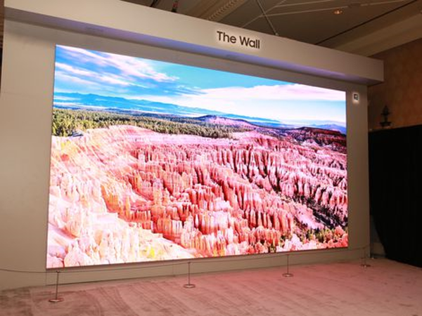
Samsung’s 2020 version of The Wall, measuring 292 inches, on display at CES. (Image: CNET)
MicroLED Televisions
- A highlight of CES was a super-size setup of The Wall measuring 292 inches (more than 24 feet, or 7.4 meters). If that’s a tad too big for your living room, The Wall also comes in 75-inch (4K), 88-, 93-, 110- and 150-inch 8K versions.
- Other large-format microLED screens included Chinese brand Konka’s 236-inch 8K TV, and LGE’s microLED display—it measures “only” 145 inches, but still delivers astonishing picture quality and detail, as do all the latest microLED television screens.
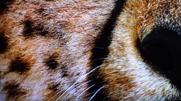
Close-up look at the fine detail around a cheetah’s nose, courtesy of LGE’s 145-inch microLED television, as displayed at CES 2020.
MicroLEDs in AR/VR/MR
CES wasn’t only about big screens, however—there were also some “micro” microLED displays to be seen, such as those intended for near-eye-display (NED) use in augmented- (AR), virtual- (VR), and mixed-reality (MR) devices. Some highlights in the NED space included:
- Swedish company glō, a spin-off from Lund University, showed 1.6- and 1.8-inch full color microLED displays. These displays are based on TFT backplanes that were built in collaboration with JDI (1.6-inch) and Kyocera (1.8-inch).2 Their booth also featured a full-color microLED-display AR/VR headset based on RGB LEDs. While not yet in use by any AR device makers, the glō approach shows promise for future development.
- Plessy showed a 1080P microLED-based near-eye-display solution for augmented- and mixed-reality devices.
- Japan’s JBD (Jade Bird Display) demonstrated microLED displays for AR/VR that are smaller than a penny, but offer extremely high brightness (up to 3 million nits).3 While 3M nits isn’t something you want to stare at with the naked eye, these microLEDs open new opportunities for optical designs that make use of transparency. They also can be extremely energy efficient, since running them even at very at low-powered “dim” levels will still provide brightness equivalent to standard diodes.
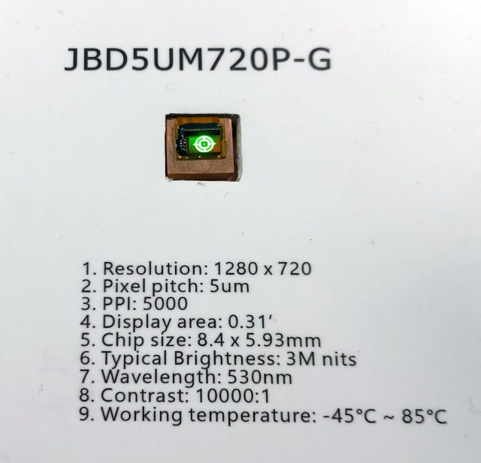
JBD’s monochromatic, extremely bright microLED display. (Photo credit: Road to VR)
As a point of interest, don’t be confused by the “micro OLED” AR/VR device introduced by Panasonic at CES, developed in conjunction with Kopin. While they are innovative, these new high-definition VR glasses are not made from some new type of microscopic-sized OLED emitters, but are rather high-grade OLED displays that are “micro” in size: i.e., they are OLED microdisplays. Likewise, some of the televisions billed as “microLED” are more accurately categorized as miniLED displays, such as TCL’s 118-inch The Cinema Wall 4K TV, and Planar/Leyard’s 216-inch The Great Space 8K television: “these so-called microLED TVs are similar to large-size RGB miniLED displays with ultra-fine pitches.”4
Other MicroLED Innovations
Meanwhile at CES, Taiwan’s Industrial Technology Research Institute (ITRI) showcased its innovative “pixel area release” technology, which integrates sensor functions into the pixels of a microLED device to adjust display brightness automatically based on ambient indoor/outdoor light conditions. ITRI has also been gaining ground in solving some of the micro LED production challenges that have so far delayed mass commercialization of the technology.
From their booth, they showed a modular microLED display that they claim is “the worlds’ first display fabricated by the use of mass transferred micro LED chips onto Printed Circuit Board (PCB) backplanes without the use of temporary backplanes.”5 This technique was developed in conjunction with PlayNitride, Inc. (who provided the microLEDs), Unimicron Corp. (the PCB backplanes), and Macroblock, Inc. (driver ICs and display assembly). ITRI says their method has the potential to reduce microLED display production costs as much as 20%.6
ITRI discusses their PCB-based microLED assembly approach.
MicroLED Commercialization Challenges
As exciting as it may be to see all these new displays at CES, the prospect of integrating microLED technology into mainstream (and affordable) consumer devices for the mass market seems to keep getting further away. Rumors that microLED smart watches might reach the market this year haven’t come to fruition yet (but stay tuned, the year is young). A display’s journey from a prototype displayed on the floor of CES to your local electronics store can be long. The latest forecast from Digitimes Research projects that large microLED displays won’t start to become widespread until 2024.
“As sizes of glass substrates are limited for production lines, it is difficult to produce LCD or OLED TV panels of over 120 inches. In comparison, micro LED display modules can be mosaicked into 110-, 220-, 440-, 790-inch or even larger displays and will therefore have market niche in commercial displays of over 100 inches.”7
DigiTimes Research's analysts forsee that “a new manufacturing process via embedding CMOS circuits in micro LED chips seems to be able to hike yield rates and thereby decrease production cost for micro LED panels. The process reduces complexity of mass transfer of micro LED chips onto backplanes to facilitate wafer-level production and testing. In addition, backplanes are not limited to TFT-LCD glass substrates and can be made of glass, metals or flexible materials.”8
MicroLED Quality Challenges
Whatever microLED fabrication methods ultimately prove effective for the yields and costs required for mass commercialization, there is a pervasive need for quality assurance throughout the manufacturing process. Radiant offers effective measurement and inspection solutions for microLEDs at the chip/wafer level and at the panel/assembly level.
Some of the microLED inspection challenges we’ve encountered—and solved—include controlling for stray light from neighboring pixel defects and removing cross-channel (color) false defects for accurate registration of individual microLED pixels and subpixels, enabling manufacturers to qualify their display components and perform LED module calibration (pixel uniformity correction). For extremely precise inspection at the individual pixel and subpixel level, Radiant’s ProMetric® Imaging Photometers and Colorimeters—when used alone or with the add-on Microscope Lens—capture and measure every display pixel with precision, regardless of subpixel layout. Typically applied for subpixel characterization in R&D and lab environments, the Microscope Lens enables the resolution of the imaging system to be applied to a very small (zoomed-in) portion of a display or wafer, for exponentially greater measurement precision at each light-emitting element (each individual microLED).
Once microLEDs are transferred to the final backplane, Radiant’s measurement systems can be used to evaluate luminance and color uniformity across the entire panel at once. The advantage of a 2D imaging photometer or colorimeter is its ability to capture a large spatial area in a single image to detect and measure all areas of nonuniformity and mura (blemishes). Ultra high-resolution imaging systems also enable all pixel-level luminance and color measurements to be captured at once within full-FOV images of the display, even without a microscope objective lens. These comprehensive measurements enable very efficient pixel uniformity testing and calculation of correction factors for display calibration in production settings.
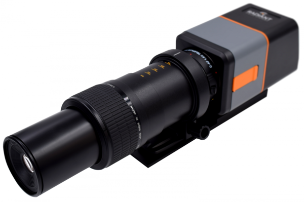
Radiant’s ProMetric® Y-Series Imaging Photometer used with our Microscope Lens, which provides 5x and 10x magnification for extremely high-resolution subpixel inspection.
CITATIONS
- Katzmaier, D., “Samsung’s ‘The Wall’ TV might be the biggest screen we’ve ever seen”, CNET, January 6, 2019
- YiningChen, “CES 2020: glo Unveils RGB MicroLED Display with 525 PPI”, LED Inside, January 21, 2020
- Lang., B., “JBD Shows Micro LED Display for AR/VR? With 3,000,000 Nits Brightness”, Road to VR, January 8, 2020.
- Han, S. and Hwang, A., “Mini, micro LED catch eyes at CES 2020”, DigiTimes, January 21, 2020.
- As quoted in: Berman, A., “ITRI Showed a Modular Micro LED Display at CES 2020”, Display Daily, Januar 17, 2019
- Berman, A., “ITRI Showed a Modular Micro LED Display at CES 2020”, Display Daily, Januar 17, 2019
- Huang, T. “Micro LED to be widely used in large displays starting 2024”, DigiTimes, January 8, 2020, quoting from the DigiTimes Research Special Report: Mini/micro LED: Challenges and opportunities in the display industry, published Monday, January 6, 2020
- Ibid.
Join Mailing List
Stay up to date on our latest products, blog content, and events.
Join our Mailing List