Inspecting and Correcting Displays as Resolution Goes Up: A Method for Improved Pixel-Level Measurement
As display resolution and pixel density increase, measuring the characteristics (luminance, chromaticity) of individual display pixels becomes more difficult for current imaging technology. For instance, the imaging system that I use to measure my display may have an image sensor boasting 29 megapixels (29MP; or around 29,000,000 pixels). Each of these image sensor pixels (tiny light-sensing or photo-sensitive elements) enables me to measure the light emitted from each pixel in a display.
The more image sensor pixels I have per display, the more image sensor pixels I can apply to measure each display pixel, the more precise and accurate my measurements will be. With 29 million pixels, it seems like I have plenty to cover the number of pixels in any display I will need to measure.
But take, for example, the first OLED iPhone smartphone from Apple—the iPhone X. Its resolution is 2436 x 1125 (or 2,740,500 pixels). At this resolution, I am only able to apply 2.70 x 2.70 image sensor pixels from my 29MP measurement system across each pixel in the display. This granularity of data per display pixel isn’t optimal. I only have a little over 7 total image sensor pixels to tell me the exact qualities of light that are produced by each display pixel, and 7 sensor pixels can’t neatly cover or isolate a single display pixel. Nowadays, the highest-end OLED iPhone (the iPhone 11 Pro Max) has a resolution of 2688 x 1242 (or 3,338,496 pixels).
Hmm…Using my same 29MP imaging system to measure this display, I am now down to 2.45 x 2.45 image sensor pixels (6 total sensor pixels) to measure each display pixel. I’m losing measurement precision over each pixel as display resolution increases (and it will only increase from here).
There are tricks I can use to increase my “effective” imaging resolution per display pixel. I can measure the display in several sections (applying my 29MP sensor resolution to fewer display pixels in a single image) and stitch multiple images of the display together to understand its overall output and uniformity. Similarly, I can illuminate subsets of pixels in the display (say, every 3rd pixel, increasing my effective resolution by 3X), measure each subset separately, and then stitch multiple images of the display together this way.
For display manufacturing, however, this doesn’t really cut it as a quality control method. It’s important to optimize display inspection efficiency to meet viable production takt times. Thus, an ideal inspection solution should use a single image of a display—applying my imaging system’s resolution to measure all of the display’s pixels at once—to perform all necessary analyses. To do this, imaging systems must continue to accurately measure an increasing number of pixels in a display while applying an increasingly limited number of image sensor pixels (relative to the resolution of a display).
Importance of Pixel-Level Measurement in Today’s Emissive Displays
The need for pixel-level measurement is a bit technology dependent, and is becoming more important as new emissive displays emerge in the market. Because these displays use individual emitters (that is, each pixel produces light independently), the pixels in OLED (organic light-emitting diode), miniLED, and microLED displays can exhibit variability in brightness and color output from pixel to pixel. This variability manifests as non-uniformity or “mura” (Japanese for “unevenness”) that is visible across the display, resulting in low yield of acceptable displays, rejection of expensive components, or costly rework. Ultimately this slows commercialization of new emissive display types because production is so costly and unreliable that yields don’t match market demands and the end-cost of devices ends up being prohibitive for consumers.
Example of non-uniform output of individual pixels on emissive displays (inset images), resulting in an uneven screen appearance to human viewers (background images): at left, a microLED display, at right, an OLED display.
Automated visual inspection of displays is a proven method to identify defects like non-uniformity, with quantitative pass-fail results, fast cycle times, and reduced operational costs necessary for mass production and commercialization. For emissive displays such as OLED, miniLED and microLED, pixel and subpixel measurement methods have enabled the calibration of display uniformity by identifying, measuring, and correcting the output of each pixel, thereby producing displays of entirely uniform appearance. This process—referred to as pixel uniformity correction, or “demura”—relies on the accuracy of pixel-level measurement to calculate accurate correction coefficients for each pixel.
Correcting Emissive Displays to Improve Yield
As display size scales, yields decline drastically, and the cost of each component is much higher. At a certain point, it becomes viable for manufacturers to perform correction (electronic compensation, or calibration) to improve display image quality. The concept is simple: by modifying the inputs to individual subpixels of an emissive display, previously identified dim pixels can be adjusted to a uniform brightness level resulting in improved uniformity and correct color across the display.
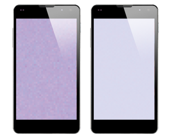
Images of an OLED smartphone screen before (left) and after (right) applying “demura” correction to improve uniformity.
Display pixel uniformity correction requires, first, having in-display electronics that can control brightness of the individual subpixels and make adjustments based on the calculated correction factors for each subpixel. Second, a measurement system is required to accurately quantify individual pixel brightness and color, and compute specific correction factors for each of them.
Demura. The demura method employs three steps:
- Measure each subpixel in the display to calculate luminance and chromaticity values at each pixel coordinate location using a high-resolution imaging system (often an imaging photometer or colorimeter). Accurate measurement values for each subpixel are essential because correction coefficients are calculated from these values.
- Load measurement data from each pixel’s coordinate position into a coefficient calculator. Correction factors are calculated to normalize luminance and chromaticity discrepancies between pixels in the display using test analysis software.
- Apply correction factors to the signals of each subpixel at each pixel location using an external control IC (integrated circuit) system.
Challenges of Pixel-Level Measurement
The demura method has been proven effective for ensuring the visual quality of millions of displays in mass production worldwide. However, ensuring measurement accuracy necessary for qualification and correction at the pixel level becomes more challenging as the resolution of emissive displays increases and pixels become smaller, more numerous, and closer together. As we discussed in our iPhone example above, display resolutions are on a constant upward trajectory. The latest smartphones contain anywhere from two- to more than four-million pixels per display (with three or four times the number of subpixels) spaced from 400-500+ pixels per inch (PPI).
Also illustrated by our iPhone example, imaging resolution versus display resolution determines the number of photo-sensing elements (sensor pixels) available to measure each individual display pixel. Applying more sensor pixels per display pixel increases the granularity of data acquired by the imaging system for accurate measurement. But, as overall display resolution increases, an imaging system’s ability to apply sufficient sensor pixels per display pixel in single-image measurement is reduced. To increase the accuracy and repeatability of pixel-level measurement values, image-based measurement systems must maximize both the number of sensor pixels across each display pixel (pixel registration) and the data captured by each sensor pixel (pixel measurement).
Registration Challenges. Pixel-level measurement relies first on accurate pixel registration, a method of dynamically setting a region of interest (ROI) that is centered on and defines the area around each display pixel in the measurement image. This technique was originally patented by US7907154B21 for the purposes of measuring individual LED pixels in large-format outdoor screens, where measurements are performed over long periods of time and multi-image measurement of a single display is common in order to optimize image sensor resolution per display pixel.
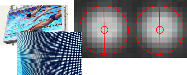
Example measurement of a large outdoor LED display screen (video wall). ROI are illustrated by the red circles on the measurement image to the right. In this case, there are so many sensor pixels (small squares) in the measurement image, an ROI that is centered on a sensor pixel “more or less” in the center of a display pixel will provide the registration precision we need for pixel-level measurement.
Here, ROI can be set as a uniform grid aligned to the image sensor array (each ROI is aligned to the center of an image sensor pixel, which is not necessarily at the exact center of a display pixel). This works in these multi-image, resolution-optimized measurement scenarios—there are so many sensor pixels across each display pixel, the ROI alignment doesn’t have to be precise to the display pixel center. Likely, aligning the ROI to an image sensor pixel will more or less center the ROI to the center of the display pixel.
However, we don’t have the luxury of multi-image measurement when it comes to quality control of smaller displays (i.e., smartphones, watches, or microdisplays). We need single-image measurement to meet production speeds—and as we’ve seen, this reduces our available sensor resolution per display pixel. Looking back at the iPhone example, with only 2.45 x 2.45 sensor pixels per display pixel to work with, it is unlikely that the center of a display pixel and the center of a sensor pixel will be aligned. This reduces the ability of the ROI to precisely cover and isolate each display pixel for measurement.
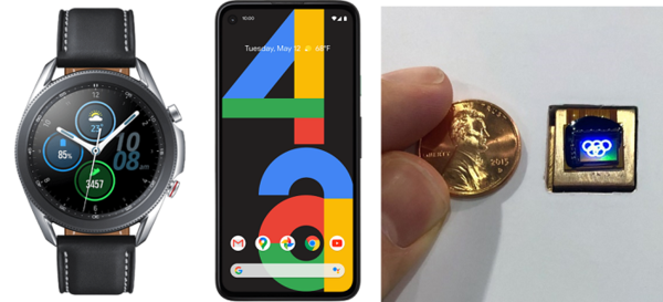
A sample of new OLED and microLED display sizes. Pixel-level measurement these displays must be both accurate and fast to ensure production efficiency. Left to right: Samsung Galaxy Watch3 with AMOLED display, Google Pixel 4a smartphone with OLED display, and a microLED microdisplay from Jade Bird Display (JBD). (Images L-R: © Samsung, © Google, © Jade Bird Display)
Measurement Challenges. Second, pixel-level measurement relies on, well, accurate pixel measurement. We need to maximize the amount of data acquired by each of the image sensor pixels that are used to cover each display pixel (the sensor pixel area of our ROI). In scenarios where we are only applying a handful of sensor pixels to measure a single display pixel, we don’t have a lot of granularity for measurement. It’s hard to understand the exact quantitiy and quality of light produced by a single display pixel when light is captured by sensor pixels whose area likely falls both inside and outside the bounds of a single display pixel’s ROI. We really only want to measure the area of the sensor pixels that is inside the ROI to understand the true value for that pixel.
What's needed is a new approach to continue to measure display pixels accurately as display resolutions increase. Answering the call, Radiant has developed a new pixel-level registration and measurement method that uses fractional image sensor pixels to improve measurement accuracy for today’s high-resolution displays.1 Particularly important is that this method now allows for effective qualification and demura of emissive (OLED, mini/microLED) displays.
The fractional pixel method first sets a display pixel ROI based on a floating-point limit to align the ROI to the center of a display pixel (rather than centering the ROI on the image sensor pixel). Then, the method isolates the fractional sensor pixel area contained within the ROI to calculate a display pixel measurement. This improves the precision of measured values within each display pixel over traditional (“whole pixel”) methods to enable accurate display qualification and correction, or demura.
The benefit of a fractional pixel method is accurate pixel-level measurement using reduced imaging resolution. We can take a single image of a very high-resolution display without losing measurement accuracy, maintaining the effectiveness of our measurement system for quality control at testing speeds.
Fractional Pixel Method
The fractional pixel method addresses measurement scenarios where imaging sensor resolution per display pixel is limited, enabling image-based measurement systems to continue to accurately measure and correct today’s high-resolution displays, even with a single-image.
Fractional Registration. The first step is optimizing pixel registration. As we’ve discussed, traditional measurement methods align ROI to the measurement system’s sensor pixel array. However, as display resolutions continue to increase relative to measurement system resolutions, it is more likely that the center of a display pixel will not be aligned with the center of a sensor pixel, reducing the ability of the ROI to precisely cover and isolate each display pixel. This misalignment can result in measurement error.
The fractional pixel method addresses this by setting the ROI as a floating point. An initial measurement image captures luminance values across the display and determines a center of gravity (highest luminance value), indicating the center of a display pixel. The ROI is centered to this value, rather than the sensor array. To illustrate this, in the image below to the right, the ROI can even be centered to the intersection of four sensor pixels based on the luminance value being highest here.
Illustration of the effect of centering a display pixel ROI to an image sensor pixel (traditional method, left) where significant area of the display pixel may be excluded from measurement, versus weighting luminance values of fractional pixels to determine the true center of the display pixel for alignment of the ROI (fractional pixel method, right).
Fractional Measurement. Second, the fractional pixel method optimizes pixel measurement. The fractional pixel method calculates pixel output values (luminance, chromaticity) based on the fractional area of each sensor pixel contained within the ROI (see the image below, on the right). This improves the precision of measured values over traditional “whole pixel” methods that factor values from the entire sensor pixel area that is only partially within the ROI (see the image below, on the left). That is, the fractional pixel method allows us to maintain measurement granularity with fewer sensor pixels across each display pixel. The fractional pixel method ensures the accuracy of pixel-level measurements using a single-image capture, maintaining quality control within takt time requirements.
Illustration of a traditional “whole pixel” measurement method versus the fractional pixel method. In the traditional method (left), display pixels are measured using 100% of the data from sensor pixels whose area is more than 50% inside the ROI, and 0% of the data from sensor pixels whose area is less than 50% inside the ROI. Using the fractional pixel method (right), display pixels are measured using a percentage of data based on the percentage of sensor pixel area inside the ROI.
The accuracy of the fractional pixel method was recently demonstrated by Radiant in a study comparing limited-resolution fractional pixel and whole pixel measurements against extremely high-resolution reference measurements of the same OLED display. In this study, the fractional pixel measurement data adhered closely to the reference measurement data, whereas the whole pixel measurement data diverged from the reference data at multiple points.2
To learn more about the fractional pixel method and see the results of Radiant’s study, read our White Paper: Fractional Pixel Method for Improved Pixel-Level Measurement and Correction (Demura) of High-Resolution Displays.
CITATIONS
- Pedeville G., Rouse J., inventors; Radiant Vision Systems LLC, assignee. Methods and systems for measuring electronic visual displays using fractional pixels. WO2019040310A1. 2019 Feb 28.
- Pedeville, G., Rouse, J., and Kreysar, D., “Fractional Pixel Method for Improved Pixel-Level Measurement and Correction (Demura) of High-Resolution Displays”, Society for Information Display (SID) Display Week 2020 Digest. Book 2, August 2020. ;
Join Mailing List
Stay up to date on our latest products, blog content, and events.
Join our Mailing List