Honey, I Shrunk the Display: Measuring Small LEDs, Pixels, and Subpixels
Today’s device displays rely more and more on small, emissive components like LEDs (Light Emitting Diodes) and OLEDs (Organic LEDs) to provide the high-resolution viewing experience that consumers have come to expect. To create these displays, manufacturers have been taking advantage of developments that provide smaller emissive elements, squeezing more and more of those elements into the same space, resulting in much higher pixel counts and much sharper images.
In the technology industry, we love our acronyms, and the key acronym here is PPI: Pixels Per Inch. The higher number of PPI, the higher the resolution of a display screen. For example, in 1998, a Nokia 5110 cell phone display panel contained 65 pixels per square inch. By contrast, one of today’s 4K televisions contains about 4,000 pixels across the horizontal dimension (thus the name “4K”).
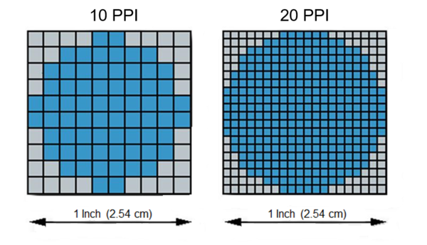
In the example above, as pixel density increases from 10 PPI to 20 PPI, the number of pixels in a square inch increases, and the size of each individual pixel is much smaller. Image credit: Scientiamobile.
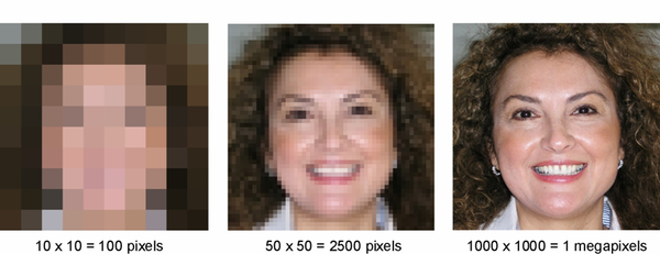
Pixel count translates into spatial resolution, which determines the clarity and detail visible in an image.
Today’s smartphone displays contain thousands or even millions of pixels. As a display’s pixel density or PPI increases, more fine details and sharper images become visible. With rising interest in miniLED and microLED displays——the need to measure minute details with precision will only continue to grow. As their names imply, miniLED and microLED displays consist of arrays of microscopic LEDs (sized in the 100-200 µm and <100 µm range, respectively), each a unique pixel. Since display quality is directly affected by its pixel-level output, there is a growing need in display design and manufacture to measure ever-smaller light-emitting elements for accuracy and to ensure the accuracy of the finished display device.
This is especially true of emissive displays like OLED, LED, or microLED, where each pixel in a display produces its own luminance, which typically results in wide variations in output from pixel to pixel. These individual variations can cause non-uniformity that is visible even at a distance, especially when viewing the display at high bright states. Pixel defects and other tiny flaws can be especially noticeable when displays are viewed close up, like those in augmented and virtual reality headsets and smart glasses.
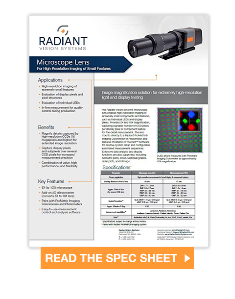
To measure pixel-dense displays and individual emissive elements, Radiant provides a specially designed lens option: our Microscope Lens. Designed for high-resolution imaging of small light source and display features, the Microscope Lens enables you to characterize extremely small components and features, such as individual LEDs, display pixels, and subpixels.
The lens attaches directly to a ProMetric® Imaging Colorimeter or Photometer, available in a range of resolution options. Used with Radiant ProMetric or TrueTest™ Software, the Microscope Lens provides a compact and efficient photometric measurement solution for controlling the visual quality of displays, small light sources, and other devices. The Lens can be used to determine accuracy of the output of pixels designed into a prototype, the pattern and shape of pixels, or to measure individual emitters chosen for particular applications.
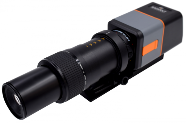
The Radiant Microscope Lens paired with a ProMetric Y-series imaging photometer.
Pixel Geometry
The individual pixel elements (the red, green, and blue diodes) in a display can be arranged in many different patterns. For example, computer monitors—which are rectangular or square—typically have pixel components arranged in vertical strips. Many smart device manufacturers employ proprietary pixel patterns to improve the visual performance of their displays as compared to their competition. Display manufactures need to be able to inspect these patterns to ensure accuracy according to the intended design.
Sample of subpixel layouts for three different OLED display screens.
Subpixel patterns like those shown in the image below can be challenging to characterize without a very high-resolution system and optics capable of microscopic measurement. The Microscope Lens provides 5X or 10X magnification of images captured by extremely high-resolution imaging systems. This high precision enables design manufacturers to ensure accurate subpixel layouts, shapes, and RGB color patterns. As shown in the picture inset, we can achieve extreme detail in a very small spatial area to properly image individual elements with a substantial amount of separation between light regions.
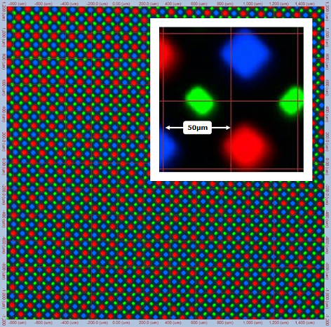
Using the Radiant Microscope Lens, we can capture extreme detail at the subpixel level to inspect subpixel geometry and patterns.
Characterizing Individual LEDs
The physical structure of LEDs (diode sources) is more complex than most other light sources. Imperfections in brightness and color can occur due to material, mechanical, or electrical defects within each emitter. Evaluation of individual LEDs can be critical for ensuring the performance of LED-based systems, and the uniformity of brightness and color when LEDs are combined in an array.
The Radiant Microscope Lens can be used to evaluate properties of LEDs alone or in an array, including:
- LED uniformity
- LED edge contrast (uniformity falloff)
- Effect of cross-talk between LEDs (undesired illumination of an LED by a neighboring LED on an array or panel)
- Cross-section plots showing LED luminance uniformity
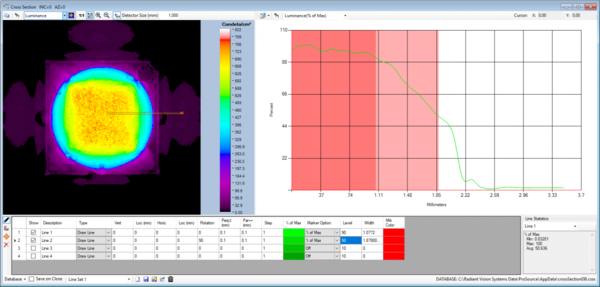
Measurement image of a single LED (left) and cross-section showing edge contrast of the LED (right), where luminance level falls off over a given distance in millimeters. Results shown in TrueTest Software.
To learn more about the Radiant Microscope Lens, download the Spec Sheet.
Join Mailing List
Stay up to date on our latest products, blog content, and events.
Join our Mailing List