Progress in MicroLED Displays
The most recent market report from DSCC analysts predicts that the microLED display market could reach $1.38 billion worldwide by 2027,1 significant growth from the current estimated $950 million2 market. Other industry analysts agree that demand for miniaturized, energy-efficient displays will continue to drive a focus on achieving microLED commercialization in the next 5-8 years.
MicroLED displays have many advantages—they offer high brightness and contrast ratio, a wide color gamut, and low energy use. They are also more durable than OLEDs, have a consistent appearance across a wide viewing angle, and provide ultra-high image resolution. How are microLED makers addressing issues such as mass transfer processes and low production yields that still stand in the way of mass market viability? This blog post looks at some recent developments and techniques that are helping move microLED displays forward.
MicroLEDs in Micro Displays
MicroLED displays have already started to take off for products like smart watches and AR/VR devices. Their small size (typically around 50 microns) is one obvious reason, but their brightness and energy efficiency are also advantages for these applications. Smartglasses and AR/MR devices display images on a transparent surface with the background environment and ambient lighting visible to a user. The brightness of microLEDs provides better contrast and visibility. The extremely high resolution of microLED displays is also an advantage for any near-eye display (NED) devices.
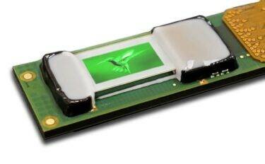
A microLED microdisplay from Plessy. (Image © Plessy Semiconductors).
One recent advancement in AR glasses comes from MICLEDI Microdisplays. They’ve come up with microLED devices with integrated micro-lenses capable of pixel-level beam shaping. So far, they’ve provided green and blue microLED test kits with the integrated micro-lenses to their customers, with red kits anticipated by the end of 2022. These devices provide “multiple benefits for waveguide-based AR glasses, including:
- Improved power efficiency – by focusing light within the targeted waveguide cone
- Optimal waveguide in-coupling – offering additional flexibility for AR system integration and image quality improvements via controllable compensation of color dispersion
- Pixel scaling to sub-3.0-micron pitch – with highly reproducible beam shape performance.”3
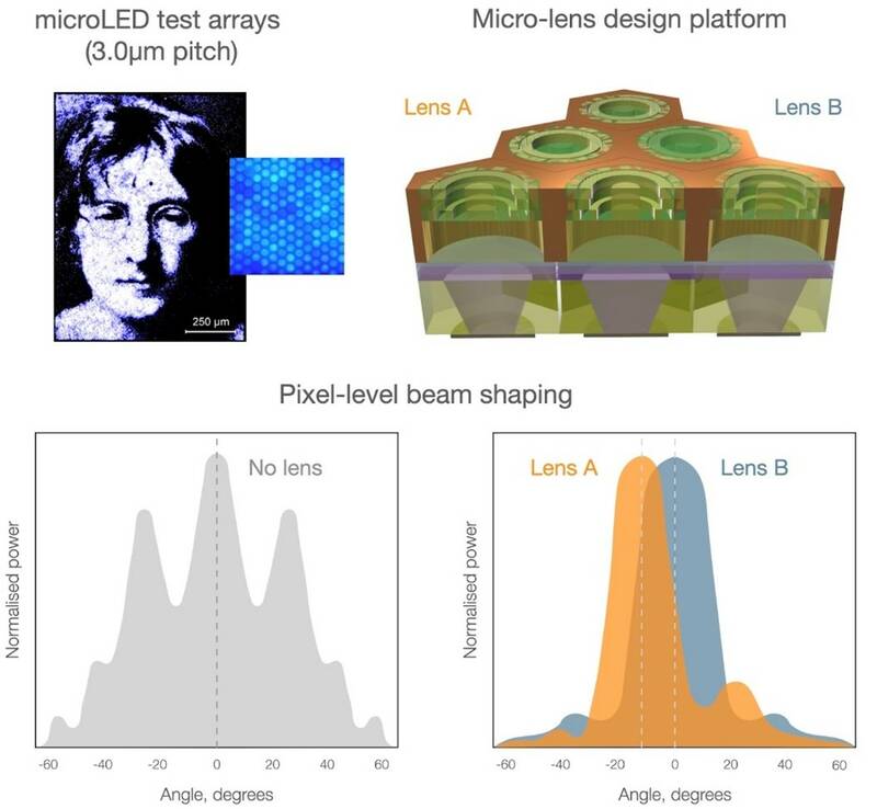
Example of pixel-level beam shaping with the microlens (right graph) compared to the more diffuse beams from a typical microLED array (left graph). (Image © MICLEDI)
Coming to a Living Room Near You?
Samsung Display set the large-scale microLED standard with the release of The Wall several years ago. Now the company has come out with a new offering for the high-end residential market called “The Wall All-In-One.” Previewed at the recent CEDIA Expo in Denver, the Wall All-In-One was designed to be set up by field installers in just a couple of hours. It comes with all the necessary parts and accessories and doesn’t require extensive structural support or ventilation, which “makes it easy for commercial customers with the old-technology LFT video walls to upgrade with the latest and greatest video performance.”4
At a price of $155,000 for the 110-inch display, this Wall still isn’t within reach of the average consumer but is already generating excitement among commercial and small business customers. CEDIA attendees also saw giant microLED screens from LG Display (136”) and Sony (220”).
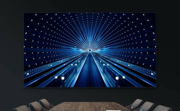
Samsung’s The Wall All-In-One 14-inch microLED display model. (Image © Samsung)
MicroLED Displays on the Road
The automotive display industry has been exploring microLED displays, which offer comparable or better brightness but better durability than OLED display panels. Brightness is a key requirement for vehicle displays that must be readable in all ambient lighting conditions from nighttime to direct sunlight. For example, PlayNitride has a new 11.6” 24:9 2480 x 960 (228 PPI) automotive-grade microLED display that provides 1,000 nits brightness.
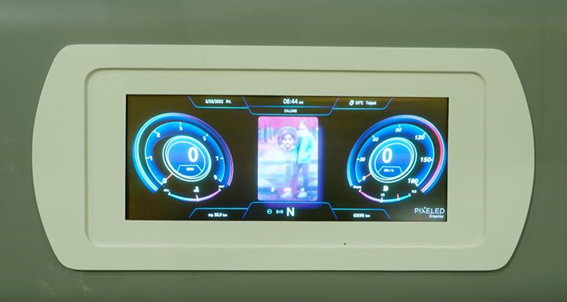
PlayNitride’s microLED automotive display shown at SID Display Week in May 2022. (Image Source)
The Mass Transfer Challenge
One of the biggest bottlenecks slowing the emergence of microLED displays is the mass transfer process. Getting millions of tiny microLED chiplets successfully mounted to a display substrate is a complex and time-consuming process. For example, a 4K 3840×2160 monitor requires more than 20 million microLEDs to be transferred to a backplane with micron-scale accuracy. How to achieve high speed and throughput volume while minimizing defects is the first problem to be solved. And then inspection and correction of any defects is the next problem.
Traditional LED stamp pick-and-place transfer processes using the MEMS array technology proved too slow. New transfer methods that show promise include:
- Static Transfer. Transfer heads release static electricity to pick up microLEDs from a carrier substrate and then release them to the target substrate. Multiple heads can be grouped together into a static transfer head array that can move large quantities of microLEDS simultaneously.
- Laser Transfer. Laser beams can be used to quickly transfer a large quantity of microLEDs from the original substrate to the target. There are several different approaches to laser transfer, including Uniquarta’s Laser-Enabled Advanced Placement (LEAP) and QMAT’s Beam Addressed Release (BAR) laser transfer release. A benefit of laser methods is that there is no mechanical contact with the microLEDs, reducing the risk of damage during transfer.
- Fluidic Assembly. In this process, millions of microLEDs are suspended in a fluid that passes over a substrate “that is populated with an array of trap sites [wells], arranged as display pixels…Once the microLEDs have settled, the suspension is forced to flow across the substrate, pushing devices across the surface and over the trap sites. Many assembly attempts occur randomly every second, thanks to numerous microLEDs and trap sites. Thus, stochastic assembly is massively parallel, and proceeds very quickly.”5
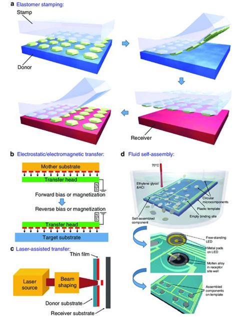
Comparison of microLED mass transfer techniques. (Image Source)
Once microLEDs have been deposited into an array, the next step is inspection to identify any defects such as inconsistencies in microLED brightness or color, dead pixels, and other issues. These defects can result in displays with a noticeable non-uniform or speckled appearance. But inspecting the millions of tiny microLED pixels requires a solution capable of extremely precise high-resolution measurement.
Quality Inspection Solutions for MicroLED Displays
Radiant offers a range of solutions and methods to address quality control at critical points in the microLED fabrication process. To provide wafer-level inspection of microLED chips, a ProMetric® Imaging Photometer or Colorimeter and TrueTest™ Software can be used with our Microscope Lens to magnify microLED subpixels at extreme detail in a measurement image.
For panel-level inspection, Radiant has developed two methods that have been proven to significantly improve an imaging system’s ability to isolate and measure increasingly small subpixels in increasingly high-resolution displays. Radiant solutions apply patented methods (US Patent 9135851; US Patent 10971044) capable of measuring all individual microLED subpixels in a display at once to calculate discrepancies between subpixel output. This enables output to be adjusted to uniform values at all display bright states—a process called pixel uniformity correction (PUC) or demura.
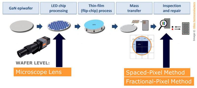
Radiant provides unique hardware and software solutions for pixel- and subpixel-level inspection at each stage of quality inspection during the microLED fabrication process, at the wafer stage inspecting individual chips, and at the panel stage following mass transfer and assembly.
To learn more, watch the webinar, Fractional Pixel Method for Improved Pixel-Level Measurement and Correction (Demura) of High-Resolution Displays.
CITATIONS
- MicroLED Display Technology and Market Outlook, Display Supply Chain Consultants (DSCC), November 9, 2022.
- MicroLED Display Market Analysis 2022, 360 Market Updates, November 10, 2022.
- “MicroLED Devices with Integrated Micro-lenses,” LED Professional, August 16, 2022.
- Tarr, G., "Wall-in-on microLED dispay packages proliferate at CEDIA Expo 2022," HD Guru, October 4, 2022.
- Schuele, P., et al., “Making MicroLED Displays with a Fluidic Assembly Process,” Compound Semiconductor, July 8, 2020.
Join Mailing List
Stay up to date on our latest products, blog content, and events.
Join our Mailing List
