CCD Sensors, Albert Einstein, and the Photoelectric Effect
Charge-coupled device (CCD) sensors are used in many of today’s advanced digital cameras and imaging systems. CCDs were first developed in 1969 by physicists Willard Boyle and George Smith. They based CCD technology on Albert Einstein’s theory of the photoelectric effect, through which light is converted into electrons. A CCD sensor captures those electron signals in the form of image points, or pixels, enabling them to be read digitally.
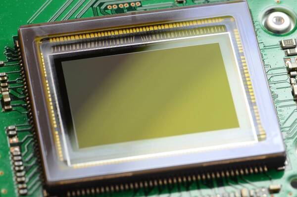
CCD sensor mounted on a circuit board.
Often called “The Fathers of Digital Photography,” Boyle and Smith were awarded the 2009 Nobel Prize in Physics for the invention of the CCD and its impact throughout technology.
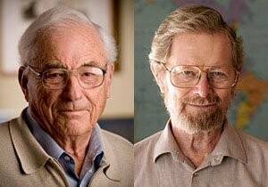
Willard S. Boyle (left) and George E. Smith, winners of the Nobel Prize in Physics for their work in digital imaging and their invention of the CCD sensor.1
Albert Einstein
If Willard and Boyle are “Fathers,” that must make Albert Einstein the “Grandfather” of the CCD camera. Einstein is one of Radiant’s Physics Heroes, and has a conference room in our corporate headquarters named in his honor.

Born in Germany on March 14, 1879, Einstein is considered the most influential scientist of the 20th century. His general theory of relativity reconciles Newtonian laws of mechanics with the laws of electromagnetics. He was awarded the 1921 Nobel Prize in Physics based on the profound impact of his work. Einstein left Europe in 1933 after being targeted by the Nazis. He became a Professor of Theoretical Physics at Princeton University, where he remained until his death in 1955.
In a seminal 1905 paper on the relationship between matter and energy, Einstein proposed that the energy of a body (E) equals the mass (M) of that body multiplied by the speed of light (C) squared, or E=MC2. This equation indicates that tiny particles can be converted into huge amounts of energy—the source of atomic power.
In 1905, Einstein also published his works on Relativity, the Special and General Theory. While it may be what he’s most famous for, the Theory of Relativity is not what earned Einstein the Nobel Prize. Rather, it was his work on the photoelectric effect.
The Photoelectric Effect
Early scientists had thought light was made of particles (Sir Isaac Newton, 1643-1727), while others theorized light was a wave (Robert Hooke, 1635 – 1703, and James Maxwell, 1831-1879). Einstein determined that light energy is carried in discrete, quantized wave packets (photons), thus light could be simultaneously a wave and a particle.
This theory resolved questions about the relationship between light of different frequencies (colors) and the energy (electromagnetic radiation) of that light. The photoelectric effect is how optical signals are converted to electrical signals, and is the fundamental process behind CCD cameras.
When light shines on a metal (or in the case of a CCD sensor, a silicon metalloid) surface, typically the energy of that light (the energy contained in the photon packets) will dislodge electrons from the surface in a phenomenon known as the photoelectric effect—also referred to as photoemission. This happens for all wavelengths of photelectric energy from 190-1100 nanometers (nm), encompassing the full spectrum of visible light, which is roughly 380-700 nm.
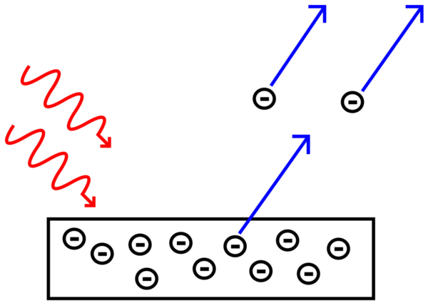
The photoelectric effect occurs when light shines on a metal surface, causing it to eject electrons (photo electrons).2
CCD Technology
When incident photons carrying a charge are absorbed by the CCD detector material, they create electron-hole pairs. During photographic exposure, the ejected electrons accumulate in individual detector elements, called the pixels or photosites of the CCD. (These are not the same pixels that emit light in a display screen). The brighter the light shining on the metal of the CCD surface, the greater the number of electrons ejected.
In essence, a CCD sensor is a slab of silicon or silicon layers, which are typically “doped” with the addition of other elements like phosphorous to alter its conductive properties. The silicon is then covered with an insulating layer of metal oxide, which lets light energy in through “gates.” These gates have a charge that allows only one-way energy transfer, trapping the electrons.
The CCD sensor is divided up into rows by channel stops, and thin aluminum strips are laid on top to form a grid. Each of the squares in the resulting grid is a pixel. As electrons are released under light exposure, they migrate up to the surface of the silicon layer and are then confined within the pixel grid.
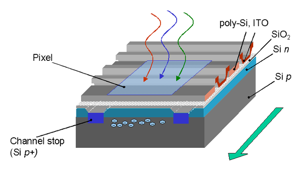
A simplified 3D cross-section of a CCD sensor with various layers of doped silicon. The shaded area on top is the pixel size, the green arrow indicates the charge transfer direction.
Once the sensor has captured the light’s electrons, it can then read the value (accumulated charge) within each pixel across the CCD. The total amount of charge (number of electrons) that accumulate in each pixel is linearly proportional to the amount of light incident upon it—the more light intensity emanating from the photographic subject, the more charge ends up stored in the pixel.
An analog-to-digital converter (ADC) then turns each pixel's value into a digital value by measuring the amount of charge in each pixel or photosite and converting that measurement to binary form. This creates what is essentially a digital, machine-readable copy of the light patterns that have fallen on the device, recreating the original image.
Alternating currents through the aluminum strips move the stored electrons row by row to the edge of the sensor, where the charge is registered and recorded in the camera’s memory. This leaves the CCD sensor empty and ready for the next photographic exposure.
A detailed discussion of the science of camera sensors, including silicon doping, the electromagnetic processes of a CCD, and various operating considerations. Skip ahead to 6:16 if you only want to hear how CCD sensors work.
Capturing light intensity with a CCD sensor produces black and white images. For color imaging, filters are used to separate the incoming light into its distinct wavelengths of color—red, green, and blue—so each can be captured and measured to recreate a full-color photographic image. Radiant colorimeters use a tristimulus filter wheel system matched to human perception (“tri”-stimulus standing for the three primary filters that are used to match the response of the three different cones in our eyes), as defined in the CIE color space.
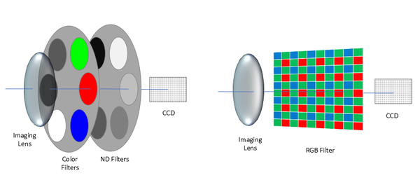
A typical Bayer-pattern RGB filter (right) provides information about intensity of light in red, green, and blue wavelength regions—but does not have the sensitivity to discriminate each individual wavelength like our eyes do. A tristimulus filter wheel system (left) uses CIE-matched color filters to replicate the human eye’s perception of light and color.
There are a few basic forms of CCD architecture with many sizes and variations for specific applications, from cell phone cameras to scientific study—for example, CCD sensors are used in the Hubble Space Telescope and for medical imaging. CCD sensors are known for their light sensitivity, color accuracy, and ability to contain a large number of pixels with high electron capacities, which yield high-resolution images. These characteristics make CCDs particularly effective when precision detail is needed to distinguish details in an image.
Radiant’s ProMetric® imaging photometers and colorimeters use scientific-grade image sensors optimized for the highest performance—with low noise characteristics, high resolution, and an extremely fast data transfer speed. To learn more about using image-sensor-based systems for precision light and color measurement, read our whitepaper, “Guide to Choosing an Imaging Colorimeter”.

IMAGE CREDITS
1. Image credit for Boyle and Smith photos: National Academy of Engineering.
2. Image credit for Photoelectric Effect: licensed under Creative Commons Attribution-Share Alike 3.0 Unported.
Join Mailing List
Stay up to date on our latest products, blog content, and events.
Join our Mailing List