Is Inkjet Printing the Answer to OLED Production Challenges?
OLED (Organic Light Emitting Diode) displays offer brighter colors, darker blacks, better view-angle performance, a faster refresh rate, and better energy efficiency than LCD displays. OLED has become common in small consumer displays such as smart phones and watches, but OLED production challenges and low yields continue to plague manufacturers of larger displays, keeping costs high most significantly for larger display products like OLED televisions.

The Samsung Galaxy S10 OLED smartphone. Image credit: Samsung.com
In recent years, research and development has focused on using inkjet printing as a production method for OLED. Several FPD (flat panel display) makers in Japan, Korea, Taiwan, and China are developing inkjet-printed OLED displays, and it appears that the technique is poised for commercial application as soon as 2020.1 Industry analysts are predicting that inkjet OLED production capacity will rise 12-fold by 2024 as more display makers master the technique and consumer product companies put more OLED devices on the market.2
Standard OLED Production
An OLED display is made by placing a series of organic (carbon-based) thin films between two conductors. When an electrical current is applied, the OLEDs (diodes) emit light through a phenomenon called electroluminescence or electrophosphorescence. Traditional LCD displays use a rigid backlight layer of white LEDs with a filter in front that determines the color shown on the display’s surface. By contrast, OLEDs are individual emitters composed of Red, Green, and Blue (RGB) elements that can display any color.
OLED displays are made of multiple layers of organic materials for optimal efficiency and performance. A typical OLED has five layers of material:
A typical OLED is made up of five layers of material; different types of OLED (e.g., passive-matrix, active matrix, white, foldable) are variations on this basic structure.3
Standard OLED production relies on a vacuum evaporation process, where organic materials are deposited on a sheet through a thin stencil (called a shadow mask). By either vacuum thermal evaporation (VTE) or organic vapor phase deposition (OVPD), the material is cooled and condensed into a thin film. In this standard process, a significant amount of material is wasted because it is deposited on the mask instead of the substrate, and contaminants and particles can be easily introduced, causing defects that result in low yields and high costs.
Inkjet Production Process
You may know inkjet primarily as a method of printing on paper. The concept of inkjet production was first developed in the 1950s, with commercial inkjet printers released on the market in the 1980s. They work by depositing miniscule droplets (between 50-60 microns in diameter) onto a sheet of paper, fired by tiny jet nozzles.
The idea behind inkjet OLED printing is essentially the same: nozzles deposit a precise amount of material onto a substrate such as glass or film to build up the pixels of a display. OLED inkjet printing offers the advantages of precise material placement without needing a mask, thus reducing waste and stray particles, and thereby increasing yields. Inkjet printing also saves time by reducing production interruptions to clean the chamber walls.
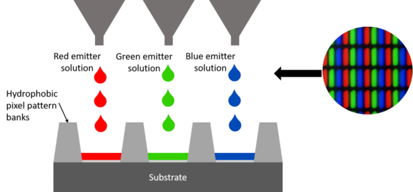
Schematic representation of printing RGB layers into subpixels for an OLED TV display.
The emergence of better OLED inks has helped speed the development of the technology. significant testing has also been required to solve challenges in the production environment and to obtain film uniformity.
Inkjet OLED printing methods hold the promise of scalability to larger screen sizes. Some manufacturers are now using a floating stage that improves accuracy of inkjet deposits over a large area. Analysts estimate that inkjet printing of a 65-inch 4K television in a Gen 10 facility would be 15-20% less expensive4 than the white OLED (WOLED) process currently used. Just this spring, JOLED, Inc. (an OLED-focused joint venture of Sony and Panasonic) announced that it has broken ground on the world’s first mass-production-line facility for printed OLED displays, located in Chiba, Japan.
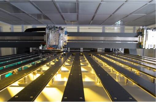
A floating stage system allows the glass substrate to float on a thin cushion of nitrogen, using pressure and vacuum simultaneously to move the glass and ensure smooth application of ink. Image source: Kateeva.
Thin Film Encapsulation
Another challenge with OLED materials is that they are very sensitive to oxygen and moisture—even a single water molecule can damage OLEDs. To prevent this, OLED layers are encapsulated, often between layers of glass. Rigid glass works well for any type of flat display, but as the industry moves toward flexible and foldable display form factors, new techniques have been developed using various films, called Thin Film Encapsulation (TFE).
Just as inkjet printing is an effective method to deposit the OLED layer of a display, it can also be used as a method to deposit the TFE layer. Pioneering OLED inkjet company Kateeva reports that its technology can now achieve mass production of TFE layers that are four microns or thinner.
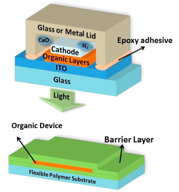
Schematic side view of an encapsulated OLED with traditional encapsulation layer (top), and thin-film encapsulation (bottom). Image: Creative Commons License CC BY 4.0 from Yu. D., et al.5
Measuring OLED Display Quality
Even with recent inkjet advancements, OLED display production still demands constant vigilance to maintain yields. Tiny contaminants (dust or fluids) can damage the OLED materials and tiny scratches or film irregularities can mar the resulting display, decreasing yields. To measure and inspect OLED displays (whether inkjet-printed or otherwise) to ensure uniformity requires a high-precision imaging system capable of detecting pixel and sub-pixel variations.
Radiant’s ProMetric® Imaging Photometers and Colorimeters can measure and quantify every pixel and sub-pixel element of an OLED display in a single measurement to evaluate luminance and ensure uniformity. Paired with TrueTest™ Software, our display metrology solution provides the combination of high-resolution and comprehensive photometric testing that’s needed to precisely measure each and every emissive element in an OLED screen.
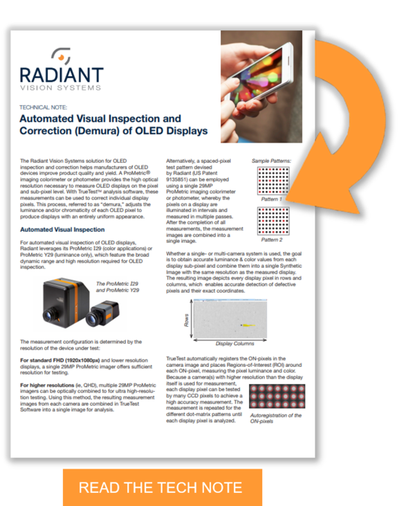
Our OLED “demura” solution even allows panel makers to correct mura (areas of non-uniform luminance and color) across the screen so that displays appear uniform for all colors and at all bright states. The result is less waste and increased yields as the corrected displays can now be sold on the market. As OLED production technologies continue to advance, Radiant’s solution engineers continue to develop innovative solutions to help manufacturers ensure quality and improve production. To learn more about our demura solution, read the tech note, Automated Visual Inspection and Correction (Demura) of OLED Displays.
CITATIONS
- Kuo, R. and Shen, S., “Commercial production of inkjet print OLED panels to realize in 2020”, Digitimes, July 19, 2020.
- OLED Mobile Phones Market Research and Analysis Report, published by Docera, September 2012
- Inkjet Printing for AMOLED Technology and Market Report 2019, by IHS Markit, July 22, 2019, as reported in O’Halloran, J. “Inket OLED displays on the verge of mass production”. RapidTVNews.com, June 29, 2019.
- Bassett, A., “OLED prices set to drop with latest production techniques”. AVForums.com, June 28, 2019
- Yu, D., et al. “Recent progress on thin-film encapsulation technologies for organic electronic devices.” Optics Communications, Volume 362: March 1, 2016, pp. 43-49.
Join Mailing List
Stay up to date on our latest products, blog content, and events.
Join our Mailing List