Innovations in OLED Technology Expand the Possibilities for Next-Gen Displays
Organic Light Emitting Diode (OLED) technology was invented by researchers at Eastman Kodak company in 1987. OLEDs are made from organic (carbon-based) semiconductor materials that emit light when they receive an electric current.
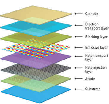
Ultra-thin layers of organic semiconductors are sandwiched between two charged electrodes, one positive, one negative. This OLED “sandwich” is placed on a substrate such as sheet of glass or other transparent material. “When current is applied to the electrodes, they emit positively and negatively charged holes and electrons. These combine in the middle layer of the sandwich to create a brief, high-energy state called ‘excitation’. As this layer returns to its original, stable, ‘non-excited’ state, the energy flows evenly through the organic film, causing it to emit light.”1

Structure of an OLED display, with the emissive diodes layered between two electrodes (cathode and anode). Movement of electrons between these layers creates energy that is emitted as light. (Image: Optics and Photonics News, Source)
A Multitude of OLED Display Applications
OLEDs have caught on due to their many advantages, including brightness, vivid color range, and energy efficiency, which have made them an appealing technology for many commercial applications. OLED panels also offer display makers unique capabilities in terms of flexibility, shape, and transparency. Because they are self-emissive, OLEDs don’t require a backlight like LCD displays, which makes OLED panels thinner, lighter, and more flexible than prior display technologies.
Display applications for OLEDs include:
- Flat panel displays (FPDs) such as televisions, smartphones, and laptops, where the brightness, energy efficiency, wide color gamut, and thinner panels appeal to consumers—although typically these displays have a higher price point than LCD and LED-backlit screens.
- Flexible display screens including curved monitors, automotive displays that mold to the contours of the dashboard, rollable displays, and the newest foldable-screen smartphone models.
- Microdisplays, including those used for smartwatches, wearable devices, and the display modules in AR/VR headsets and smartglasses.
- Transparent displays, which are used often for digital signage in public and retail locations.

Clockwise from upper left: BOE’s curved “Smart Dashboard” automotive display, the Samsung Galaxy® Z Fold 3 foldable phone from Samsung, the popular Alienware® curved gaming monitor from Dell, LG Display’s rollable TV that rises from its box for viewing then rolls back down out of sight, a transparent OLED display from LG, and a Fitbit™ wearable device with OLED microdisplay. (Images © Samsung, © Dell Computers, © LG Display, and © Fitbit.)
With all these different applications and use cases, it’s not surprising that the OLED display market is expanding rapidly. In fact, it’s projected to almost double from US$38.4 trillion in 2021 to nearly $73 trillion in 2026 (a CAGR of 13.6%).2
An OLED-on-silicon microdisplay from Kopin, for use in mobile VR devices. (Image Source)
New OLED Technology Advancements
Research and development in academia and commercial firms continues to expand the capabilities of OLED technology and help it to find new applications today and in the future. Some recent OLED innovations include:
- The worlds brightest OLED microdisplay – eMagin recently revealed the prototype for the world’s first full-color OLED microdisplay with luminance exceeding 10,000 cd/m2 (candela per square meter, aka nits). Using a new full-color patterning technology, the prototype offers 1820x1200 pixels within a 0.87-inch (22.1 mm) diagonal microdisplay. Designed to appeal to “makers of military, medical, and industrial AR/VR headsets, thermal scopes, night vision goggles, aircraft helmets, and similar applications,”3 the displays will be fabricated by eMagin in house. The company is aiming to achieve a display with 28,000 nits brightness by 2023.
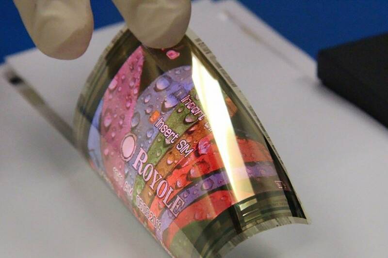
- Ultra-thin OLED displays – manufacturers and buyers of televisions are enthusiastic about the thin profile possible with OLED displays. Because they have no backlight or LCD layers, OLED screens can often be just 2-3 mm at their thinnest point. The thinnest screen on the market currently is LG’s aptly named “Wallpaper” OLED TV at just 0.15 inches (3.81 mm) thick. Ultra-thin OLEDs are also necessary for making flexible/foldable display form factors. Component maker Royale created the first ultra-thin rollable OLED panel at a mere 0.01 mm thick, and Pioneer now offers durable OLED panels at 0.1 mm thick for use in flexible and bendable devices.

Prototype of Royale's ultrathin (0.01 mm) rollable OLED microdisplay. (Image Source)
- Applying AI to Improve OLED Materials – one challenge that has dogged OLED displays and slowed their adoption, especially in more rugged environments such as outdoor digital signage and in automobiles, is that it can have a shorter lifespan than LCD or other display technologies. This is mainly due to the blue organic material. But Cambridge, Massachusetts-based Kebotix has announced it will be ready to start testing novel blue emitters with device makers in 2022. The company applied AI and machine learning approach to analyze a pool of 20 million molecules per week to identify the few that hold potential to increase yields, lower fabrication costs, and improve the lifetimes of blue emitters. It has identified several dozen candidates that it will be testing with various device makers.
Inspecting and Correcting OLED Displays to Improve Yield
As OLED products have moved beyond the research lab and into production, commercial viability of the technology depends on maintaining product performance and quality while also controlling manufacturing costs. To minimize waste and ensure high production yield, OLED display manufacturers rely on visual inspection systems to detect and correct defects.
High-performance imaging colorimeters such as Radiant’s ProMetric® I-series can accurately measure the luminance of individual pixels and subpixels in an emissive display and enable manufacturers to evaluate overall display uniformity. Radiant also provides a complete solution for correcting display uniformity—a process called demura (removing “mura” or blemishes).
The Radiant demura solution employs three distinct steps:
- Measurement of each subpixel in the display to calculate luminance values at each pixel location (performed on different test images to measure each series of same-colored subpixels) using a high-resolution imaging colorimeter.
- Calculation of correction factors needed to normalize luminance discrepancies between subpixels in the display using test analysis software.
- Application of correction factors to the display signals using an external control IC (integrated circuit) system to adjust output at each subpixel.
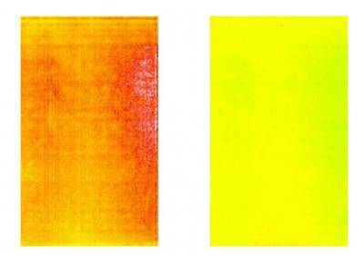
When our demura correction process is applied to a finished OLED or microLED display, there is a significant improvement in visual quality of the display. The net effect of demura is that displays that would have failed quality inspection without electronic compensation will now be able to pass, thereby reducing waste in manufacturing, improving cost efficiency, and increasing production yield.

Measurement images of a blue test screen on an OLED display, before and after demura correction (shown in a false-color scale in Radiant TrueTest™ Software to illustrate luminance levels).
To learn more about automated visual quality inspection and correction of OLED displays, read the whitepaper “How to Use Imaging Colorimeters to Correct OLED, MicroLED, and Other Emissive Displays for Improved Production Efficiency and Yields,” or watch the webinar, "OLED Pixel Measurement and Correction."


Preview of Coming Attractions
The next breakthrough OLED product could be Samsung’s newly announced OLED quantum dot television, which could be released as soon as 2022. There have been so-called “QLED” TVs on the market for several years, but these are made with a quantum dot (QD) layer over a traditional LCD display.
Samsung’s new “QD Display” television will likely be the first commercial product to combine OLEDs and quantum dots. It will not use direct-view QD technology but will be a QD/OLED hybrid, according to early reports.4 QD maker Nanosys suggests that it could use a bright layer of blue OLEDs with a QD filter layer to convert some pixels to red and blue. But we’ll have to wait to hear from Samsung to confirm the details. Stay tuned…
CITATIONS
- Bellis, M., “OLED Technology Guidelines and History,” Thought Co., August 14, 2019.
- OLED Market with COVID-19 Impact Analysis by Product (Smartphone, Television Sets, Smart Wearables, Large Format Displays), Panel Type, Panel Size, Technology, Vertical, and Geography – Global Forecast to 2026. Markets and Markets, March 2021.
- Werner, K., “Color OLED Microdisplay Exceeds 10,000 Nits,” Display Daily, November 15, 2021.
- Morrison, G., “Samsung’s QD-OLED TV might be here very soon. Here’s everything we know,” CNET, November 9, 2021.
Join Mailing List
Stay up to date on our latest products, blog content, and events.
Join our Mailing List
