MicroLED on the Cusp
MicroLED (µLED) is on the forefront of emerging display technology. Production challenges have slowed the progress of development and kept costs too high for the mass market, so microLED devices haven’t reached commercialization yet, with the exception of a few very high-end displays. But manufacturers are getting closer and closer to releasing small and mid-size microLED display products for consumers in the next couple of years.
What are MicroLEDs?
A microLED is a light emitting diode (LED) typically <100 micrometers (µm) square, with <50 µm common, and some falling in the 3–15 µm size range. For scale, microLEDs are roughly 1/100 the size of a conventional LED, or about 1/10 the width of a human hair. In a microLED display, each pixel (each diode) is individually addressed and driven to emit light without needing a backlight, (similar to OLED displays), but they are made from inorganic materials and offer a longer lifespan (similar to LEDs).
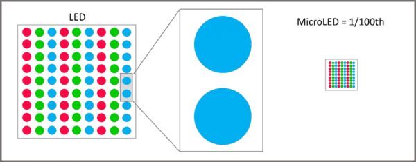
Illustration showing the comparative scale of traditional LEDs (inset) and microLEDs.
MicroLED Advantages
These tiny LEDs offer the potential of wider color gamut, contrast ratio, and deeper blacks than LCD (liquid crystal display) and OLED (organic light emitting diode) displays. MicroLEDs match OLED technology for response time and view-angle performance, but exceed OLED in brightness and ruggedness, with much lower power consumption.
MicroLEDs have a maximin pixel per inch (PPI) of 5,000 with 105 nits, compared to 3,500 PPI and ≤2 x 10³ nits for OLEDs, according to LG Display.1 And like OLEDs, microLEDs can be deposited on different substrates including glass, plastic, and metal to enable flexible, bendable, and foldable displays.
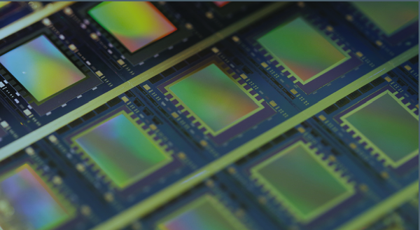
Active matrix microLED micro-display chips on a 4-inch wafer, fabricated using JBD’s monolithic hybrid integration technology. (Image © JBD)
MicroLED Applications
As the demand for higher and higher resolution displays continues, microLEDs are poised to be the next breakthrough technology in the industry. MicroLEDs are particularly appealing for devices such as smart watches, head-up displays (HUD), and augmented reality (AR) displays where high luminance and resolution are particularly important for visual performance in small spaces, at close proximity to the eye, or under variable ambient lighting conditions.
Samsung has already launched microLED display televisions. The current (2019) market for microLEDs themselves is estimated at $170 million,2 with 43.5% compound annual growth rate (CAGR) projected through 2029.3
Producing an entire television screen out of microLED chips has so far proven to be challenging. Currently, the largest-size microLED display module falls at 12 inches due to low yield.4 Larger-sized panels are usually manufactured by splicing the small ones.
For example, despite its maximum 292-inch screen size (corner to corner), Samsung’s microLED television—“The Wall”—is actually made up of multiple LED modules (roughly 6” x 6” square) arrayed together like tiles on a uniform canvas.
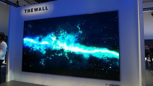
Samsung’s large-format microLED display, The Wall (Image: TechRadar)
To make a single full-size 8K display would require roughly 100 million microLEDs assembled, with zero errors, at a throughput speed of >100 million units/hour. Developers are working hard at bringing production accuracy up and costs down, and there are prototype devices in existence, but microLED-based consumer products are not expected to reach the general market until at least 2020.5 As “technology builders continue to work on improving the yield of mass transfer and bonding . . . inspection and repairing are also still bottlenecks for Micro LED mass production.”4
MicroLED Production Challenges
MicroLEDs are typically made from inorganic gallium nitride (GaN) LED materials, which create brighter displays (many times brighter than OLED) with much greater energy efficiency than traditional LEDs. However, due to their size, microLEDs require entirely new production assembly technologies, different die structure (smaller dies to enable greater control and uniformity), and new manufacturing infrastructure.
For commercialization, fabricators must find methods that yield high quality with microscopic accuracy while also achieving mass-production speeds. A microLED screen is composed of millions of tiny pixels in chip form, each of which contains some combination of red, green, and/or blue subpixels. The first phase of microLED production is wafer creation, requiring high-yield epitaxial growth.
To fabricate a display, each individual microLED chip must then be transferred to a substrate or backplane that holds the array of units in place. The transfer equipment must have an extremely high degree of precision, with placement accurate to within ±1.5 µm.
Because traditional chip bonding and wafer bonding processes (e.g., flip-chip, pick-and-place) don’t provide efficient mass transfer for microLEDs, various thin-film-transfer (TFT) technologies are also being explored. New transfer solutions are under development, including fluid assembly, laser transfer, elastomer and electrophotography transfer, roller transfer, and others.
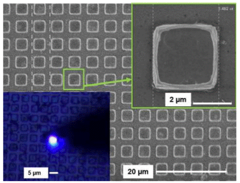
SEM micrograph of 3-µm size / 5-µm pitch microLED array fabricated with direct bonding approach. Inset lower left is an optical photograph of microLED switched on. (Image Source: Leti1)
MicroLED Quality Inspection
Manufacturers typically are looking at quality at several stages in the development of a microLED display: from LED chip and wafer through module, panel, and final device assembly. At the individual LED level, in many cases luminance and color output must be so precisely measured that a microscope lens (a microscope objective) may be needed, paired with a photometric or colorimetric device to ensure precise specifications are met.
Developers are racing to find production solutions that deliver cost-effective performance to exceed customer expectations for viewing experiences. Defects, variations in color or brightness, and other irregularities can quickly deflate buyer satisfaction, hurt brand reputation, and erode market share. If these issues cannot be addressed and corrected at the component level, low yields and high production costs will impede the viability of microLED display technologies for the mass market.
To ensure the absolute quality of microLED display devices, Radiant’s measurement solutions–including PRoMetric® Imaging Photometers and Colorimeters used alone or with our Microscope Lens—are enabling MicroLED manufacturers to asses display performance and uniformity down to the subpixel level, with accurate and repeatable results. Advantages of our solutions include:
- High-resolution measurement – our new ProMetric Imaging Photometers incorporate scientific-grade sensors that deliver an unparalleled balance of high-resolution and low noise. Our proprietary moiré removal technique eliminates this aliasing effect without sacrificing resolution by defocusing the measurement image, or other imprecise methods.
- Human color perception – Replicating the human eye’s response is critical for measuring display color accurately. Radiant’s imaging systems apply CIE color-matching functions using tristimulus color filters for colorimetric measurement to provide the most relevant evaluation of color as it will be perceived by users of a device. When measuring individual emissive elements like microLED subpixels, systems with Bayer mosaic (RGB) color filter arrays fall short. These RGB systems are not closely matched to CIE color-matching functions and therefore do not tolerate the variability in color across millions of microLED subpixels when calibrated to a single point, thus they do not provide the same accuracy on a pixel-by-pixel basis.
- Low noise – Image noise (which can include read noise, shot noise, or electronic noise), interferes with the clarity of the image. No matter how high the resolution of an imaging system (the number of megapixels of its sensor), if the system has a low signal-to-noise ratio, or SNR, then its ability to characterize the luminance or color output of the display accurately and repeatably—especially in an area as small as one pixel—can be negatively impacted. Radiant systems are engineered with low noise for improved image clarity.
- Test and analysis tools – our TrueTest™ Software for automated visual inspection enables multiple display tests to be run in sequence for rapid in-line quality control or inspection. It includes a full suite of quality tests and defect detection tools, including analyses for luminance, color, uniformity, pixel defects, contrast, gradient, points of interest, and mura.
- Demura – Radiant offers powerful tools to inspect and correct display mura to help manufacturers improve product quality and increase yield. Our patent-pending “fractional pixel” method enables manufacturers to accurately measure emissive displays such as OLED and microLED with arbitrary resolutions, well beyond the resolution of the measurement system. Then, they adjust the luminance and/or chromaticity of each subpixel to produce displays with an entirely uniform appearance. Radiant’s demura solution quantifies the exact correction coefficient to address pixel-level non-uniformity, and is adaptable for various pentile structures, moiré patterns, and gamma inconsistency.
A 1.5-inch, 264 ppi microLED display on an LTPS backplane, from glō, could be coming soon to a smart watch near you. (Image: glō)
CITATIONS
- Lapedus, M., “MicroLEDs: The Next Revolution in Displays?”, Semiconductor Engineering, May 29, 2019.
- Global (United States, European Union and China) MicroLED Market Research Report 2019-2025, published by Industry Research, July 25, 2019.
- “GaN micro-LED market to grow at 43.5% CAGR to 2023, driven by displays”, Semiconductor Today, September 2, 2019.
- Chen, Y, “Micro LED and Mini LED Opportunities in the Oversupplied Display Market”, LEDinside, September 6, 2019
- Moore, S., “MicroLED Displays Could Show Up in Products as Soon as 2020”, IEEE Spectrum, July 22, 2019.
Join Mailing List
Stay up to date on our latest products, blog content, and events.
Join our Mailing List