Imaging Colorimeters: A Critical Component of OLED and MicroLED Commercial Production
Organic light-emitting diodes (OLED) and microLEDs (μLED) are emerging as the next wave of technology in the display market. Display screens based on these emissive layers promise improved performance and visual appearance with greater efficiency than other display technologies, thanks to their individually driven pixel elements.
Both OLEDs and microLEDs have superior contrast ratios and sharper images, with deeper blacks and more vibrant colors, than traditional LCDs. Because each pixel is its own emitter, these displays require no backlight, resulting in thinner, lighter-weight displays that use less electricity. OLEDs also bring a dramatic boost in responsiveness, about 1,000 times faster than existing technologies, virtually eliminating blur on fast-moving and 3D video. MicroLEDs match OLED technology for response time and view-angle performance, but exceed OLED in brightness and ruggedness, with even lower power consumption.
OLED and MicroLED Production Challenges
However, high costs due to material prices and manufacturing yield issues have hindered widespread adoption of these display technologies. Thus far, OLED has been chosen for mainly small-screen displays such as smart phones and AR/VR headsets, but its use in larger panels such as televisions and large-format screens has been limited (or at least very expensive). MicroLED has only been sold commercially in modular panels to create very high-end, large-format displays such as Samsung’s “The Wall” (now available up to 292 inches in size) or Sharp’s “The Canvas” (with a maximum brightness of 2,500 cd/m2).
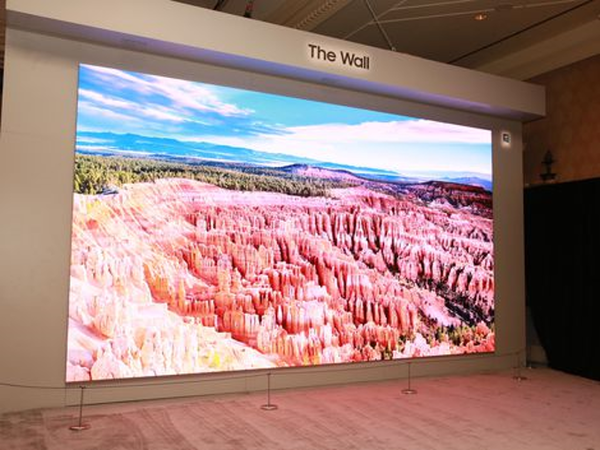
Samsung’s 292-inch version of The Wall modular microLED display shown at CES 2020. (Image: CNET)
OLED screen manufacturing has been costly to date due to inefficiency of deposition methods for adding organic molecules to their substrate (with the exception of the latest efficient inkjet printing methods). MicroLEDs require new assembly technologies, die structure, and manufacturing infrastructure. For commercialization, fabricators must find methods that yield high quality with microscopic accuracy while also achieving mass-production speeds.
OLED and MicroLED Quality Inspection Challenges
Inspecting OLED and microLED displays is in many ways more challenging than inspecting LCDs. Traditional LCD displays using LED backlights produce a mostly uniform luminance (brightness) and color output across the display screen. Any variations or defects can be measured using standard 2D photometric imaging system.
With emissive display types, however, every individual pixel in the display is subject to a high a degree of variability. For instance—although microLEDs are technically a type of LED—traditional binning processes are virtually impossible for microLEDs, which can be as small as 1/100th the size of a conventional LED.
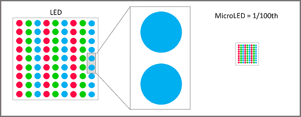
Scale representation of microLEDs compared to traditional LEDs. MicroLEDs are generally defined as being less than 100 micrometers (µm) square, with some as small as 3 µm.
Without these controls in place, ensuring brightness and color uniformity in microLED displays can be extremely challenging. It is necessary to be able to measure and quantify every pixel and subpixel element of an emissive display to identify defects and ensure uniformity, to produce the level of quality that consumers expect at these displays’ higher price points. Visual quality issues that can mar performance and consumer experience of a display device include defects like mura, nonuniform brightness, and variations in color resulting from inconsistent luminance output of each subpixel (red, green, or blue).
Inspecting and Correcting Emissive Displays to Improve Yield
Imaging colorimeter systems offer a solution to improve the quality of emissive displays. Applying scientific-grade imaging for light and color metrology, these automated inspection technologies provide an accurate measurement of display visual performance that matches the human eye’s perception of brightness, color, and spatial (or angular) relationships. High-performance imaging colorimeters such as Radiant’s ProMetric® I-Series can accurately measure the luminance of individual pixels and subpixels in an emissive display as well as evaluate overall display uniformity.
Beyond simply identifying and quantifying OLED and microLED defects using imaging colorimeters, Radiant provides a complete solution for correcting display uniformity—a process called demura (literally a process of removing mura, or “de-mura”). The Radiant demura solution employs three distinct steps:
- Measurement of each subpixel in the display to calculate luminance values at each pixel location (performed on different test images to measure each series of same-colored subpixels) using a high-resolution imaging colorimeter.
- Calculation of correction factors needed to normalize luminance discrepancies between subpixels in the display using test analysis software.
- Application of correction factors to the display signals using an external control IC (integrated circuit) system to adjust output at each subpixel.
Radiant has patented several innovative methods for increasing measurement resolution and precision for pixel-level display testing and uniformity correction, ensuring each step of the demura process is performed effectively (see: US9135851B2 and WO2019040310A1). When our demura correction process is applied to the finished OLED or microLED display, there is a significant improvement in display visual quality. The net effect of demura is that displays that would have failed quality inspection without electronic compensation will now be able to pass, thereby reducing waste in manufacturing, improving cost efficiency, and increasing production yield.
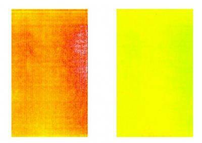
Measurement images of a blue test screen on an OLED display, before and after demura correction (shown in a false-color scale in Radiant TrueTest™ Software to illustrate luminance levels).
Learn more about how imaging colorimeter systems help safeguard manufacturing investment in OLED, microLED, and other emissive displays in this recent article published concurrently by OLED-Info and MicroLED-Info. In it, we describe the demura method of using imaging colorimeters for automated visual display measurement and correction, which enables manufacturers to calibrate their displays on the production line and achieve accurate uniformity in luminance and color.

Join Mailing List
Stay up to date on our latest products, blog content, and events.
Join our Mailing List